クレステックは徹底したマーケットイン志向の電子線描画技術を専門としたナノテク企業です
Products
CABL-UH(130kV)series

There is less forwardscatter of EB resist due to higher acceleration voltage. CABL-UH model has more accuracy less than 10nm. You can select 90kV, 110kV or 130kV due to your budget.
Beam diameter: <1.6 nmΦ
Accerelation Voltage: 130 kV, 110 kV or 90 kV
Stage size: 8 inch wafer (you can use any other wafers less than 8 inch wafer)
Special Features
◆ Vacc: 130kV Max (25-130kV, 5kV steps)
◆ Single-Stage Acceleration capability up to 130kV to minimize EOC size
◆ Micro-Discharge Free Electron Gun
◆ Beam Diameter: >1.6nm
◆ Electrostatic Lens between emitter and anode is designed to achieve very low aberration and short-rang
crossover image at the center of blanking electrodes
◆ Ultra-stable write capability is achieved using dual thermal controllers
Specifications
| Electron Emitter/ Acceleration voltage |
TFE (ZrO/W)/25 to 130kV |
|---|---|
| Min. beam diameter | 1.6nm |
| Scan method | Vector scan (x, y) (Standard) Vector scan (r, θ), Raster scan, Spot scan (Optional) |
| Advanced lithography functions (Optional) |
Field size modulation lithography, axial symmetry pattern lithography |
| Field size | sq. 30μm, sq. 60μm, sq. 120μm, sq. 300μm, sq. 600μm, sq. 1000μm |
| Work piece size | 4,6,8inchΦ (work pieces of other sizes and other shapes can be mounted with our flexible contrivances) |
| CAD software | Dedicated CAD (Standard), GDS II conversion (Optiional), DXF conversion(Optional) |
| OS | Windows |
CABL-AP(50kV)series
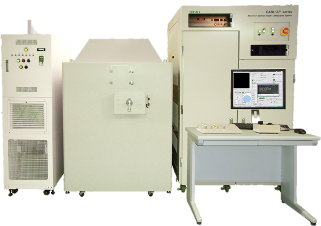
It is the best model for production of DFB-Laser diode for optical communication devices and for Academic and R&D as well. We realize high resolution and high throughput with 50kV.
Beam diameter: < 2 nmΦ (for Academic and R&D)
< 4 nmΦ (for Production)
Accerelation voltage: 50kV, 30kV
Stage size: 4 inch, 6 inch ,8 inch wafer model
Special Features
◆ TFE 50kV
◆ High resolution as same as 100kV
◆ High accurate stitch writing for long time by specially designed laser interferometer
◆ Multi-user environment (PC controlled EOC = Recipe)
◆ Self environment control - Thermal & noise free
◆ Flexible writing methods (vector, vector R-theta, raster, spot, axial symmetrical, field size modulation,
multi-mode, 3D)
User's Voice : City University of Hong Kong
Specifications
| Electron Emitter/ Acceleration voltage |
TFE (ZrO/W)/5 to 50kV |
|---|---|
| Min. beam diameter | 2.0nm (for Academic and R&D) 4.0nm (for Production) |
| Scan method | Vector scan (x, y) (Standard) Vector scan (r, θ), Raster scan, Spot scan (Optional) |
| Advanced lithography functions (Optional) |
Field size modulation lithography, axial symmetry pattern lithography |
| Field size | sq. 30μm - sq. 1000μm (50kV) (for Academic and R&D) sq. 30μm - sq. 1500μm (50kV) (for Production) |
| Work piece size | 4,6,8inchΦ |
| CAD software | Dedicated CAD (Standard), GDS II conversion (Optional), DXF conversion (Optional) |
| OS | Windows |